
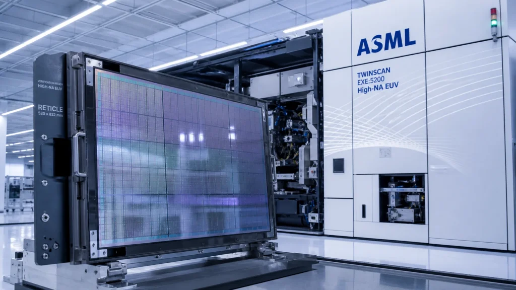
ASML said it plans to work with major chipmaking customers so its newest High-NA extreme ultraviolet tools can print the large data-center chips designed by Nvidia and others, Reuters reported from San Francisco dated Sept. 7 and published into Tuesday.
Today’s widely used EUV tools can print a chip up to about 800 square millimeters — a ceiling Nvidia, Google, and others already hit. High-NA EUV prints finer features but currently uses a smaller mask, which limits how big a chip those machines can make. Intel is already using ASMLs newest tools for laptop chips; ASML said it plans to move to a larger mask size so High-NA systems can make chips as large as today’s biggest data-center dies.
That shift is meant to spur high-volume use beyond Intel. TSMC said this week it plans High-NA in advanced-node high-volume production from 2030, while Samsung and SK Hynix are targeting High-NA for DRAM mass production around 2028, with SK Hynix evaluating a consortium on 12-inch masks. ASML plans to show a pilot line with the larger masks by 2031 and have the technology ready for high-volume production by 2033. CTO Marco Pieters told Reuters that if the industry pulls it off, productivity of those systems could rise by about 40%.
Bloomberg separately framed the move as ASML, TSMC, Samsung, and Intel backing larger masks for AI chips. This is a tooling roadmap story, not a new GPU launch.